|
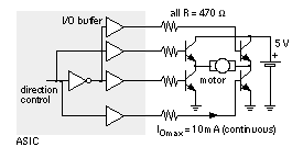
[ Chapter start ] [ Previous page ] [ Next page ] 6.1 DC OutputFigure 6.1 shows a robot arm driven by three small motors together with switches to control the motors. The motor armature current varies between 50 mA and nearly 0.5 A when the motor is stalled. Can we replace the switches with an FPGA and drive the motors directly?
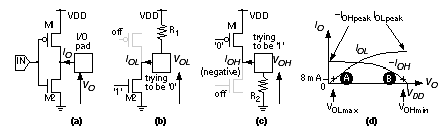
Figure 6.2 shows a CMOS complementary output buffer used in many FPGA I/O cells and its DC characteristics. Data books typically specify the output characteristics at two points, A (V OHmin , I OHmax ) and B ( V OLmax , I OLmax ), as shown in Figure 6.2 (d). As an example, values for the Xilinx XC5200 are as follows 1 :
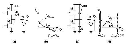
By convention the output current , I O , is positive if it flows into the output. Input currents, if there are any, are positive if they flow into the inputs. The Xilinx XC5200 specifications show that the output buffer can force the output pad to 0.4 V or lower and sink no more than 8 mA if the load requires it. CMOS logic inputs that may be connected to the pad draw minute amounts of current, but bipolar TTL inputs can require several milliamperes. Similarly, when the output is 4 V, the buffer can source 8 mA. It is common to say that V OLmax = 0.4 V and V OHmin = 4.0 V for a technology—without referring to the current values at which these are measured—strictly this is incorrect. If we force the output voltage , V O , of an output buffer, using a voltage supply, and measure the output current, IO , that results, we find that a buffer is capable of sourcing and sinking far more than the specified I OHmax and I OLmax values. Most vendors do not specify output characteristics because they are difficult to measure in production. Thus we normally do not know the value of I OLpeak or I OHpeak ; typical values range from 50 to 200 mA. Can we drive the motors by connecting several output buffers in parallel to reach a peak drive current of 0.5 A? Some FPGA vendors do specifically allow you to connect adjacent output cells in parallel to increase the output drive. If the output cells are not adjacent or are on different chips, there is a risk of contention. Contention will occur if, due to delays in the signal arriving at two output cells, one output buffer tries to drive an output high while the other output buffer is trying to drive the same output low. If this happens we essentially short VDD to GND for a brief period. Although contention for short periods may not be destructive, it increases power dissipation and should be avoided. 2 It is thus possible to parallel outputs to increase the DC drive capability, but it is not a good idea to do so because we may damage or destroy the chip (by exceeding the maximum metal electromigration limits). Figure 6.3 shows an alternative—a simple circuit to boost the drive capability of the output buffers. If we need more power we could use two operational amplifiers ( op-amps ) connected as voltage followers in a bridge configuration. For even more power we could use discrete power MOSFETs or power op-amps. 6.1.1 Totem-Pole OutputFigure 6.4 (a) and (b) shows a totem-pole output buffer and its DC characteristics. It is similar to the TTL totem-pole output from which it gets its name (the totem-pole circuit has two stacked transistors of the same type, whereas a complementary output uses transistors of opposite types). The high-level voltage, V OHmin , for a totem pole is lower than VDD . Typically V OHmin is in the range of 3.5 V to 4.0 V (with VDD = 5 V), which makes rising and falling delays more symmetrical and more closely matches TTL voltage levels. The disadvantage is that the totem pole will typically only drive the output as high as 3–4 V; so this would not be a good choice of FPGA output buffer to work with the circuit shown in Figure 6.3 . 6.1.2 Clamp DiodesFigure 6.4 (c) show the connection of clamp diodes (D1 and D2) that prevent the I/O pad from voltage excursions greater than V DD and less than V SS . Figure 6.4 (d) shows the resulting characteristics. [ Chapter start ] [ Previous page ] [ Next page ] | ||


 Animation, 3D Art and 3D Models")